Lots of stuff on this sort of issue here, and I don't wish to start needless new threads. That said, the VAST majority of the discussion is from the fall of 2009, nearly 4 years ago.
I've built the shield, downloaded and imported FAT16s WaveHc library, uploaded and put in an SDHC chip with a properly configured and 8.3 named .wav file. I get the following when I run the daphc.pde program:
Wave test!
Free RAM: 655
Card init. failed!
SD I/O error: 1, 0
I ran it both 4MHz and 8MHz; here's how it looks:
if (!card.init(true)) { //play with 4 MHz spi if 8MHz isn't working for you
//if (!card.init()) { //play with 8 MHz spi (default faster!)
putstring_nl("Card init. failed!"); // Something went wrong, lets print out why
sdErrorCheck();
while(1); // then 'halt' - do nothing!
I have not (yet) gone digging for old SD chips, a dongle and an old XP machine running FAT16. I'm using a 4GB SDHC chip and formatted it FAT32 with the SD Formatter 3.1 program released by the SD Assoc. It did not offer me the option of FAT16. I have no problem playing the file on other computers or dumb devices.
Wave Shield kit 1.1 and FAT32 SDHCs
Moderators: adafruit_support_bill, adafruit
Please be positive and constructive with your questions and comments.
-
adafruit_support_bill
- Posts: 88144
- Joined: Sat Feb 07, 2009 10:11 am

Re: Wave Shield kit 1.1 and FAT32 SDHCs
Sounds like you are not even talking to the card. Post photos of the front & back of the shield. Also, what model of Arduino are you using this with?
-
wiremanflash
- Posts: 14
- Joined: Thu Mar 14, 2013 10:36 pm
Re: Wave Shield kit 1.1 and FAT32 SDHCs
uh,,, after I solder those 5 wire jumpers in, uh, maybe I'll take a pic or 2....
just for informational purposes though, is either FAT32 or SDHC a factor at this stage of rev's? I'm using a new Uno.
-
adafruit_support_bill
- Posts: 88144
- Joined: Sat Feb 07, 2009 10:11 am
Re: Wave Shield kit 1.1 and FAT32 SDHCs
WaveHC should talk to SDHC and Fat32. But from the error messages, you are not even communicating with the card. The jumpers are a good start  . If you have more issues, post them here!
-
wiremanflash
- Posts: 14
- Joined: Thu Mar 14, 2013 10:36 pm
Re: Wave Shield kit 1.1 and FAT32 SDHCs
- 1364431010496.jpg (26.14 KiB) Viewed 1052 times
my soldering looks lame because I only had .064 xersin multicore, and plenty of flux rosin is present. I went over it closely w a magnifying glass. No cold joints or solder bridges, device polarities re-re-re-checked (pretty clear to start with).
same exact error message as when I had left out the 5 jumper wires.
- Attachments
-
- 1364431047895.jpg (22.9 KiB) Viewed 1052 times
-
- 1364431072021.jpg (23.17 KiB) Viewed 1052 times
-
adafruit_support_bill
- Posts: 88144
- Joined: Sat Feb 07, 2009 10:11 am
Re: Wave Shield kit 1.1 and FAT32 SDHCs
Can't see a lot of detail in the photos. A little larger would help (800x600 is a good size).
Some of the solder joints on IC4 look a little suspect. Review this tutorial and re-work any joints that are not smooth and shiny or have not flowed well onto both the pin and the pad. http://learn.adafruit.com/adafruit-guid ... n-problems
Also take a close look at the solder joints on the SD card holder. These are common causes of communication problems with the card.
-
wiremanflash
- Posts: 14
- Joined: Thu Mar 14, 2013 10:36 pm
Re: Wave Shield kit 1.1 and FAT32 SDHCs
not the kind of reply I like to make.... and this doesn't seem to be the place,,, but,,,,,,
I decided to quick order another 2 shields, build 'em, use some better solder, lighting, etc., and KEEP THINGS MOVING! but the site doesn't wanna let me login to order, just exactly like last time, and ada doesn't do telephones, and you tech guys here are appearing to be the only life at ada.
I wanna use a bunch of these to make a bunch of something and get paid for it,,, but I'm about to bolt. Can you do me any good?
-
adafruit_support_bill
- Posts: 88144
- Joined: Sat Feb 07, 2009 10:11 am
Re: Wave Shield kit 1.1 and FAT32 SDHCs
The store & shopping cart seem to be running OK from here. If you send a message to [email protected] with a link to this thread they should be able to get you logged on to place an order.
-
wiremanflash
- Posts: 14
- Joined: Thu Mar 14, 2013 10:36 pm
Re: Wave Shield kit 1.1 and FAT32 SDHCs
Thanks that did it. (for ordering a couple boards) This is the quickest most responsive forum on the entire Internet.
-
adafruit_support_bill
- Posts: 88144
- Joined: Sat Feb 07, 2009 10:11 am
-
wiremanflash
- Posts: 14
- Joined: Thu Mar 14, 2013 10:36 pm
Re: Wave Shield kit 1.1 and FAT32 SDHCs
I also got R6 and R8 swapped somehow. had to snip out R6, due to it's horrendous position (actually touching IC4), so I've gotta run pick up a 100k for R8 (now that I've moved it). I'm wondering though if damage might have occurred, if the purpose of R8 is substantial current or voltage limiting.
My new board (I only soldered 1 up so far) works just fine.
What are the (possible) purpose of the open positions for LED1 and LED2? I see that R9 and R10 are their series resistors,,,, probably around 300 ohms???
My new board (I only soldered 1 up so far) works just fine.
What are the (possible) purpose of the open positions for LED1 and LED2? I see that R9 and R10 are their series resistors,,,, probably around 300 ohms???
-
adafruit_support_bill
- Posts: 88144
- Joined: Sat Feb 07, 2009 10:11 am
Re: Wave Shield kit 1.1 and FAT32 SDHCs
Damage would be extremely unlikely with R6 & R8 swapped.
LED1 and LED2 can be used for any purpose. Some use it to indicate SD card activity (similar to the logger shield). 300 ohms should work fine for current limiting.
LED1 and LED2 can be used for any purpose. Some use it to indicate SD card activity (similar to the logger shield). 300 ohms should work fine for current limiting.
-
wiremanflash
- Posts: 14
- Joined: Thu Mar 14, 2013 10:36 pm
Re: Wave Shield kit 1.1 and FAT32 SDHCs
So, perhaps the most important facts yet on this thread, and perhaps findable by the search:
#1 - Wave Shield 1.1 specifically works far better than rev 1.0 BECAUSE it uses an 74AHC125N by TI (as "IC4") to provide the 3.3v power with a strong enough buss (and fast enough rise times) to properly function with SDHC chips. This is in fact the biggest change from rev 1.0.
#2 - Do not believe the very first line of
http://www.ladyada.net/make/waveshield/solder.html
,,, even though it is meant to be helpful to avoid trouble!!! At least at the present time it has a nasty typo, and the chip is INCORRECTLY named! It is in fact a 74AHC125N (as "IC4"). This is kind of like passing out a thousand business cards with a phone number only 1 digit off....
#3 - The WaveHC library and example Sketches may be better than the library it replaces, but it is still confusing, and full of comments written as wisecracks and indirect observations.
#4 - You do NOT need to load the entire WaveHC LIBRARY at the beginning of every WaveHC SKETCH
#5 The WaveHC Sketches and Libraries are overflowing with stuff, features if you will, that really should be "pruned away" for many, if not most, applications.
-
wiremanflash
- Posts: 14
- Joined: Thu Mar 14, 2013 10:36 pm
Re: Wave Shield kit 1.1 and FAT32 SDHCs
And yet more items regarding rev 1.1 and "the Wave Shield webpage" (http://www.ladyada.net/make/waveshield/) and its pages. This stuff should probably be dealt with.
regarding:
http://www.ladyada.net/make/waveshield/design.html
the text showing a date of: May 17, 2011 20:07 (same date and timestamp for instructions for "version 1.1 of the kit")
The 2nd paragraph of the page tells us that there's a 3.3v regulator, and that it's the easiest thing to understand,,,, bbbbut, 5 paragraphs later the innocent reader is told about 4 nonexistant resistors used to give us a reduced voltage instead of 5v. The next paragraph tells us about another resistor and a diode that's not in my kit, nor allowed for on my board.
But I keep on reading.
- the image of an SD chip clearly shows 7 contacts
-When I look at my board I count 8 solder pads for SD card connections, 3 for the card holder functions, and 4 soldered tabs on the shell of the holder (which sure ought to be connected to Gnd).
-the section "SD / MMC Card holder calls out:
--2 "mechanical" ground
--1 logic ground
--DAT1
--DAT2
--DATA_OUT
--DATA_IN
--SCLK
--CS
which adds up to 9.
What on earth?!?!?!???
So I go and dig up a few SD cards I have, and interestingly enough, the ones I have are quite unlike the image, having 9 connection pads (2 of which share a detent, presumably making them the "mechanical" grounds). What on earth is that thing in the picture, and from whence did it come?
I think I know what this unusual term "mechanical ground" refers to, but I don't understand how it differs from "logic ground", certainly on this particular board.
I had to go to Wikipedia and scratch through several possibilities to figure out what this "MMC" term scattered throughout the webpage might possibly have been about.
Educationally speaking, it's interesting to know about the 3 pins used for card holder functions, but it might be nice to mention (as done on the "Make it!" page) that those pins and functions are unused on this shield.
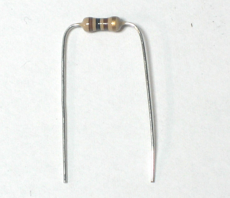
At this point I'm even going to offer to take a pic of a resistor of the correct size and values to use as R6, and formed into a "staple", so it can be posted in the img frame along side your text frame dealing with installation of R6 on the board on http://www.ladyada.net/make/waveshield/solder.html. (instead of http://www.ladyada.net/images/conway/staple.jpg).
If I seem to be going on a bit, it's sure not the kind of stuff I entertain myself with. I'm just trying to make sense out of what should be a bit better documentation. When a hardware rev comes out, documentation needs rev's (and competent proofreading) too,,, at least within a year or so!
regarding:
http://www.ladyada.net/make/waveshield/design.html
the text showing a date of: May 17, 2011 20:07 (same date and timestamp for instructions for "version 1.1 of the kit")
The 2nd paragraph of the page tells us that there's a 3.3v regulator, and that it's the easiest thing to understand,,,, bbbbut, 5 paragraphs later the innocent reader is told about 4 nonexistant resistors used to give us a reduced voltage instead of 5v. The next paragraph tells us about another resistor and a diode that's not in my kit, nor allowed for on my board.
But I keep on reading.
- the image of an SD chip clearly shows 7 contacts
-When I look at my board I count 8 solder pads for SD card connections, 3 for the card holder functions, and 4 soldered tabs on the shell of the holder (which sure ought to be connected to Gnd).
-the section "SD / MMC Card holder calls out:
--2 "mechanical" ground
--1 logic ground
--DAT1
--DAT2
--DATA_OUT
--DATA_IN
--SCLK
--CS
which adds up to 9.
What on earth?!?!?!???
So I go and dig up a few SD cards I have, and interestingly enough, the ones I have are quite unlike the image, having 9 connection pads (2 of which share a detent, presumably making them the "mechanical" grounds). What on earth is that thing in the picture, and from whence did it come?
I think I know what this unusual term "mechanical ground" refers to, but I don't understand how it differs from "logic ground", certainly on this particular board.
I had to go to Wikipedia and scratch through several possibilities to figure out what this "MMC" term scattered throughout the webpage might possibly have been about.
Educationally speaking, it's interesting to know about the 3 pins used for card holder functions, but it might be nice to mention (as done on the "Make it!" page) that those pins and functions are unused on this shield.
At this point I'm even going to offer to take a pic of a resistor of the correct size and values to use as R6, and formed into a "staple", so it can be posted in the img frame along side your text frame dealing with installation of R6 on the board on http://www.ladyada.net/make/waveshield/solder.html. (instead of http://www.ladyada.net/images/conway/staple.jpg).
If I seem to be going on a bit, it's sure not the kind of stuff I entertain myself with. I'm just trying to make sense out of what should be a bit better documentation. When a hardware rev comes out, documentation needs rev's (and competent proofreading) too,,, at least within a year or so!
-
adafruit_support_bill
- Posts: 88144
- Joined: Sat Feb 07, 2009 10:11 am
Re: Wave Shield kit 1.1 and FAT32 SDHCs
Thanks for the feedback. We are in the process of updating most of our tutorials as we move them to the Adafruit Learning System. http://learn.adafruit.com/
Please be positive and constructive with your questions and comments.