Hi guys,
I've generated gerber outputs for my PCBs and realized that there are lots of areas where the exposed copper is covered by silkscreen, potentially preventing solderability. I know that some fabrication houses automatically subtract the (inverted) soldermask layer from the silkscreen layer but many don't and I'd like to have a general solution to this problem.
http://sourceforge.net/tracker/?func=de ... p_id=33921 suggests that this feature has already been requested for gerbv and Gerbtool already has this feature but the latter seems to be very complicated and I'm clueless how to do layer subtraction.
(Please don't suggest me to include less layers upon generating my gerber files because there are some layers that are very useful and I want them all to be included.)
Thanks in advance!
Laci
Subtracting the soldermask layer from the silkscreen layer in gerber files
Moderators: adafruit_support_bill, adafruit
Please be positive and constructive with your questions and comments.
-
mondalaci
- Posts: 5
- Joined: Wed Dec 08, 2010 12:25 pm
-
westfw
- Posts: 2010
- Joined: Fri Apr 27, 2007 1:01 pm

Re: Subtracting the soldermask layer from the silkscreen layer in gerber files
Move the text and modify the silkscreen so that it doesn't cover exposed copper?
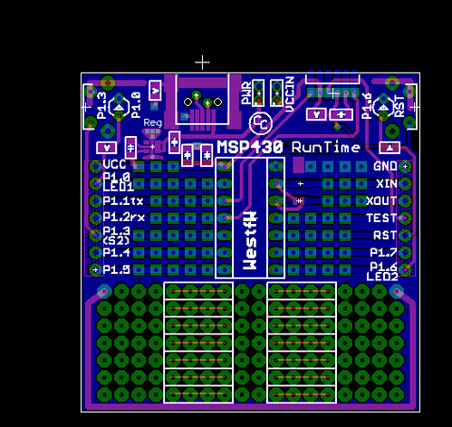
When I get serious about making a PCB look pretty (which is actually hardly ever), I use one of the silkscreen line re-sizers (I think the latest is silk_gen.ulp) (assuming EAGLE.) Aside from ensuring that the line widths in the silkscreen are all of sufficient width, this copies all of the silkscreen elements to a new layer, where they become INDIVIDUALLY EDITABLE. Edit, move, delete, resize, to your heart's content, and then use THAT layer to generate your silkscreen gerber instead of the normal combination of tPlace, tNames, tValues...
For example, here's the normal silkscreen for a MSP430 breakout board:
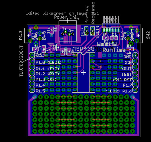
And here's the result after the process described:
When I get serious about making a PCB look pretty (which is actually hardly ever), I use one of the silkscreen line re-sizers (I think the latest is silk_gen.ulp) (assuming EAGLE.) Aside from ensuring that the line widths in the silkscreen are all of sufficient width, this copies all of the silkscreen elements to a new layer, where they become INDIVIDUALLY EDITABLE. Edit, move, delete, resize, to your heart's content, and then use THAT layer to generate your silkscreen gerber instead of the normal combination of tPlace, tNames, tValues...
For example, here's the normal silkscreen for a MSP430 breakout board:
And here's the result after the process described:
-
mondalaci
- Posts: 5
- Joined: Wed Dec 08, 2010 12:25 pm
Re: Subtracting the soldermask layer from the silkscreen layer in gerber files
Thanks for the tip, but I won't do this way. I have dozens of SMD diodes on my board and their silkscreen (which also partially covers the pads) is pretty useful for getting their polarity right. The (official) part itself is messed and I won't do any manual work. Automatically clipping the gerber file would be the ultimate solution but I couldn't find any way to do it. I think I'll just use a fab house that clips the silkscreen.
Please be positive and constructive with your questions and comments.